Search This Blog

Monday, December 25, 2023

MP2307 Buck Converter Module

I ran into some problems with a MP2307 Buck converter module recently, so I did some research on my own.

Vertically mounted modified MH-Mini-360

Here is a copy of Mini-360 schematic (.pdf) I found.


It is closed to the 3.3V output schematic in the datasheet with a few component values changed.  A variable resistor R1 was added to allow for voltage adjustment.

MP2307 is a synchronous buck converter without a low power mode.  The PWM still runs at a fixed frequency with a continuous inductor current about 1A peak to peak - positive and negative inductor current averages to zero. The negative current returns the energy to the power source. A large enough input capacitor could help to recycle the energy.

This is contributing to the high quiescent current that many have observed.

Datasheet shows Switching waveform at No Load

Richtek AN033_EN "Buck Converter Selection Criteria" talks about PSM vs PWM at low loads.


Here is a comparison of the efficiency at low load:

PSM has some disadvantages:

I have ran into low frequency switching noise of PSM interfering with my analog circuits in one of my projects.  

I used the MP2307 modules in my analog circuits as the PWM even at low load makes it easier to filter the switching noise.  See  Audio sw - Analog power supply - using as a charge pump for negative rail for analog circuits.

I have modified a module as the constant voltage/constant current charger circuit recently.


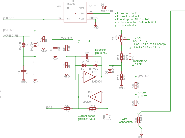
I used D4 to block current leaking from the battery during soft-start and when the input supply is disconnected. An external feedback voltage divider is connected to the battery after D4 to compensate for the diode drop.  

Battery charging current is monitored by R28.  A small DC offset of ~50mV is added so that current flowing in and out of the battery can be monitored.  The charge current is controlled by the current feedback loop at U2B. As the DC offset could be switched off for power management outside of charging making U2B output positive. D7 and D11 is used to clamp the output below the 6V limit of the MP2307.  D7 value was empirically determined as it is different than what LTSpice predicts - inaccuracy in my zener diode model.

Everything works exactly as I designed except for the Mini-360 module was overheating.  At a first glance, the MP2307 internal switch should be good enough.


Both the inductor and the MP2307 gets very hot.  The overall efficiency was around 70%. Could it be fake chips, fake inductor or something else?

It turns out, the inductor value is too low for the high duty cycle in my application.  For each switching cycle, the 10uH inductor have longer time to reach much higher current.  Both inductor and internal switch have to operate at a higher currents and cause more conduction losses.

Here is what can happen (C) when an inductor goes into saturation.  The inductor current increase more rapidly and this causes even more conduction losses at the internal switches and inductor.  

A higher inductance would have a slower rise in current.

Current vs Time plot as an inductor goes into saturation
Source: http://elm-chan.org/works/lchk/report.html

The datasheet even has an equation for the needed value:

L = 15V / (340kHz * (0.3 * 1A)) * (1 - 15V/18V) = 24.5uH, picking the next value up as 27uH.
Inductor rating is ~ 1.3 * I, so 1.3A is fine.

I only have CD75-100M inductor (10uH). I took off the wires and counted the turns 16T.

Since L is proportional to N^2, the required turns = 16T * sqrt(27/10) = 27T. I used AWG 29 wires I got from old transformer.

The core can only handle so much flux before it goes into saturation.  That flux is  proportional to N*I
2.3A * 16/27 = 1.36A which agrees with the 27uH part rating which means that it is made using the same core with more windings.

The overall efficiency went up to the 90% range after the inductor change..

At 90% efficiency, 15V*0.8A * (100% - 90%) = 1.2W for the module to dissipate.
I might charge current 0.8A (due to previous overheating) back to 1A after some more testing.

I mounted the module vertically so that its back side ground fill is also exposed.  This increases the surface area for natural convection and help with the heat dissipation.

Here are the modifications I have made.


Tuesday, December 19, 2023

Isolated power supply 2

There are primary side sensing converters e.g. LT5373 that uses the flyback pulse during the off period to regulate the output voltage. They have an article on this: Primary-Side Sensing Takes Complexity out of Isolated Flyback Converter Design.


I took a DIY approach using a regular boost converter and adding my flyback pulse sensing circuit.  The flyback pulse is rectified across C2. Q1 is a current source that is used to translate the voltage to the feedback pin across resistor R2 thus regulating the voltage across C2.   The current source is also a dummy to keep the boost converter running.

D1, C2 and R3 looks similar to the snubber used in a typical flyback converter and also functions as one.


I used the LT1961 as a simulation model because of the same switching frequency to the MT3608.  Value of R2 is changed for the higher reference voltage.


I noticed negative high voltage spikes during startup in LTSpice simulation.  These spikes goes away as the secondary side load increases as voltage ramps up.


I use a clamping diode on the switch pin to ground. The BAV99 diode comes with a second diode and is used for that purpose in my design.


The output has a PI filter consists of a small ceramic capacitor, a ferrite bead and a bulk tantalum capacitor.  At1.2MHz switching frequency, the ferrite does a good job of filtering out these ripples.

Green trace: voltage across ceramic capacitor before the ferrite bead
Red trace: voltage across tantalum capacitor after the ferrite bead

This circuit isolation is limited by the  PCB spacing as well as the enamel on the magnetic wires between the primary and secondary side.  Here is the layout on a 0.8" x 0.815" (20.3mm x 20.7mm) single sided PCB.


This circuit has good line regulation but poor load regulation unlike the LT5373.  A secondary side LDO would help.  

No load voltage: 7.45V. Full load (40 ohms) voltage: 6.51V +/- 0.01V between input voltage of 12V to 18V.  The wall wart that this module is replacing has a no load voltage 7.8V and 6.74V at 40 ohms load.


Sunday, April 30, 2023

USB Power Bank

 I got one of those Leed's USB power bank from my apartment building during a planned power outage.  It blew up when I tried to charge it.  There wasn't a whole lot I could reverse engineered from the dead parts. There was a 5-pin and a 6-pin chips and a bunch of passives. My understanding is that it uses an inverting buck boost converter for both charging and output as the VUSB pins of both the USB connectors are connected together.

I finally got around to rebuild it from scratch this weekend with what I have on hand.  The parts I have were from aliexpress before the big chips shortages. I use a LTC4054 Li-ion charger chip and a MT3608 boost converter. 

The charging rate is limited by heat dissipation on a tiny single sided PCB.  The output current is limited by the Schottky diode, inductor and battery discharge rate to about 1A (or slightly higher) or so matching to the original power bank.  


Power bank schematic

Q1 and the 1M pull down (R3) is used to invert the logic level of my switch to drive the Boost converter Enable pin.  The switch is also used to connect the R2 from the voltage divider feedback to the ground.  RGB LED is used as for Charging/Operating indicator.  


The converter goes into a PFM (Pulse Frequency Modulation) power saving mode for low current loads.
I used Green LED as they have the highest efficiency.  It is connected across the inductor to reduce idle power.  It only get energized only when the boost converter is supplying current to the load.  The brightness is proportional to load.  Fancy!


Your USB power bank might have a detection circuit that shuts itself off.  I could have used a low power microcontroller that wakes up every hundreds of milliseconds to detects voltage drop across the Schottky diode to turn on the converter.

The idle current is about 200-300uA while maintaining a 5V output when the external USB device not drawing power.  That seems high, until you realize that it'll take thousands of hours before the battery is drained.    

Power bank PCB

My PCB is taped to the existing stripped down PCB.  I had to cut the VBUS trace between the USB connectors.  The blue wires are for the RGB LED.

Populated PCB (I only have 1A/20V Schottky diode.)

I modified the USB A connector to include a contact switch that is grounded when the USB A is plugged in.    This is used to enable the boost converter circuit.

Modified connector to sense presence of USB plug

Red LED = Charging

Green LED = Operating.  Brightness proportional to load

Yellow is when both are connected, but that doesn't usually happen as the connector spacing is too closed together.

Tuesday, February 14, 2023

STM8 - Generating 2 phase PWM

A push pull converter uses two drivers that are 180 degrees out of phase.

It is possible to generate PWM on 2 channels that are 180 degrees out of phase in  TIM1on a STM8S003.  All the register settings are from the reference manual, but you won't find an example.

TIM1 is set up as an up/down counter in Center-aligned mode. This spaces out the 2 phase PWM signal evenly.

Since the timer is counting both up and down in 1 PWM cycle,  auto-reload value for TIM1 should be set as 1/2 of the value to generate PWM frequency. I used TIM1_FREQ of 27kHz in my code.

#define CPU_CLOCK 16000000UL
#define TIM1_FREQ 27000L
#define TIM1_PSCR 1
#define TIM1_CLK (CPU_CLOCK/TIM1_PSCR)
#define TIM1_ARR (TIM1_CLK/TIM1_FREQ/2)
#define TIM1_PSCRH ((TIM1_PSCR-1)>>8)
#define TIM1_PSCRL ((TIM1_PSCR-1)&0xff)
#define TIM1_ARRH ((TIM1_ARR)>>8)
#define TIM1_ARRL ((TIM1_ARR)&0xff) 

// Clk = 16MHz
CLK->CKDIVR = 0;
 
TIM1->PSCRH = TIM1_PSCRH;
TIM1->PSCRL = TIM1_PSCRL;
TIM1->ARRH = TIM1_ARRH;
TIM1->ARRL = TIM1_ARRL; 

// TIM1 enable, Center-aligned mode 3
TIM1->CR1 = TIM1_CR1_CEN|TIM1_CR1_CMS; 

Output enable (and polarity) bits of the corresponding TIM1 channels can be set in TIM1 CCERx.  I use CH3 and CH4.

// CH3, CH4 output enable, polarity active high
TIM1->CCER2 = TIM1_CCER2_CC4E|TIM1_CCER2_CC3E;

From the Reference Manual:

110: PWM mode 1 - In up-counting, channel 1 is active as long as TIM1_CNT < TIM1_CCR1, otherwise, the channel is inactive. In down-counting, channel 1 is inactive (OC1REF = 0) as long as TIM1_CNT > TIM1_CCR1, otherwise, the channel is active (OC1REF = 1).

PWM Mode 1 when ARR =8 and CCR = 4

PWM mode 2 works similarly, but with the output polarity inverted.

111: PWM mode 2 - In up-counting, channel 1 is inactive as long as TIM1_CNT < TIM1_CCR1, otherwise, the channel is active. In down-counting, channel 1 is active as long as TIM1_CNT > TIM1_CCR1, otherwise, the channel is inactive. 

One can generate a PWM signal using a sawtooth wave and a comparator.  


PWM generation using analog circuit - Sawtooth wave and a comparator

The modulating signal level is the CCR value, the TIM1 counter is the sawtooth wave. The PWM modes 1 and 2 are just the polarity setting on the comparator.


PWM generation using TIM1

 One of the TIM1 channel (CH3) is set up with PWM Mode 1 while another channel (Ch4) as PWM Mode 2.

// CH3: PWM mode 1, preload, output
TIM1->CCMR3 = (6<<4)|TIM1_CCMR_OCxPE;
// CH4: PWM mode 2, preload, output
TIM1->CCMR4 = (7<<4)|TIM1_CCMR_OCxPE;

Use PWM Mode 1 for one of the channels to center an output around Timer count = 0 and Mode 2 on the other to center around Timer count = ARR. This is how you can generate the 2 phase PWM signals.

The CCR values could be set independently. In some applications, you want them to have the same PWM duty cycles. The granularity of the PWM signal is 2 TIM1 clocks. (125ns in my code)

void Set_PWM(uint16_t Value)
{
Value >>=1;
// CCR3 = n/2
TIM1->CCR3H = Value >>8;
TIM1->CCR3L = Value & 0xff;

// CCR4 = TIM1_ARR - n/2
Value = TIM1_ARR - Value;
TIM1->CCR4H = Value >>8;
TIM1->CCR4L = Value & 0xff;
}

Turn on the MOE (Main Output Enable) bit in TIM1 BKR (Break Register). An external signal can be used to disable the TIM1 outputs in the case of a hardware fault. e.g. over-current or over-temperature condition

// Master output enable
TIM1->BKR = TIM1_BKR_MOE;

This are some the output of PWM waveform at 27kHz captured on my logic analyzer.

2 phase PWM at 27kHz

Set_PWM(2) - 27kHz close to 0% duty cycle

2 Set_PWM(294) - 27kHz close to 50% duty cycle

Sunday, February 12, 2023

Optocouplers

Optocouplers are some of those things that are deceivingly easy to a beginner, but also hard to use correctly.  If you are reading the datasheet carefully, you are in for a big surprise.

CTR (Current Transfer Ratio): sensitivity of the coupler - the ratio of the transistor output current vs the LED current.  e.g. for a 50% CTR, you have to drive the LED with 10mA and the transistor switches 5mA.

The CTR spec is very loose and likely this series of optocouplers are just different bins of the same parts.  They don't even include a max value.  


This ones show both min and max value from 100% to 200%. The following shows the part to part variation of a for a small samples of a (different) optocoupler.

CTR of a small sample of PS2021 optocoupler

Analog feedback

The optocoupler is commonly used as an analog feedback in an isolated power supply.  The error voltage is pass back as a current sink or source to close a negative feedback loop of a regulator across a voltage barrier.

I played around with the isolated power supply design from previous blog with feedback from the secondary side.  The voltage regulation is very tight and virtually stays at around 5V from 5mA to125mA load.

I have no idea on how well it would work with the loose CTR specs.

Passing digital signals

They are one of those things that was made with compromises. In order to make the device sensitive, they made a big photo-transistor at the expense of large parasitic capacitance (Millar Capacitance) and and suffers from slow speed.


Reference: Vishay has a great app. note on Faster Switching from Standard Couplers.  It covers all the technical stuff.

It'll be pretty sad day if I don't try to make something slow to go fast. I played around with LTSpice and came up with something that is not covered by the app. note.  

The values I used are determined by the optocoupler CTR.

Optocoupler circuits: simple, medium and complex

To see their performance, I put them side by side and feed each of these circuits with the same 5 pulses of 100kHz signal (200kbps data rate).


Top trace: Input (cyan), bottom traces outputs from optocoupler circuits

Simple coupler circuit (green)


CBC  (base collector capacitance) aka Millar Capacitance. It slows down the transistor. Datasheet typically uses 10V and a load resistor of 100R as their test circuit.  CBC is low at higher voltages and the small pull up value help with the rise time.

Note: the scale from Low to high (left in log scale) is very different from High to low (right in linear)

The speed is much slower when you use a large pull up resistor and lowering the voltage. The values I picked is might be useful for low data rate may be lower  tens of  kilobits per second. e.g. asynchronous serial.  It should only be used with a Schimtt Trigger input to clean up the slow rise and fall time.

The middle circuit (blue)

The optocoupler is the first stage of inverter that drives a  transistor of a second stage inverter.  Its output range is clamped to a diode drop of the transistor base voltage. The operating point is not a good spot for low CBC. 

Input (Cyan), Q1 base voltage (Purple), Output (Blue)

In spite of that, it only take about 100mV change in base voltage for the transistor to turn on or off.  It is a good compromise to squeeze an extra bit of bandwidth out of the old optocoupler. There is a bit of inconsistency in the timing. A timing analysis should be made for setup/hold time for protocols that require coordination of multiple signals e.g. SPI.

The more complex circuit (Red)

It bypasses the Miller effect as it uses the transistor junction as a photo diode. The comparator threshold is set to about mid point of the input (~100mV). The speed (propagation around 500ns) is limited by the $0.20 LM393 type of comparator that is used to amplify the signal.

You can speed up the photodiode even more by using a transimpedance amplifier.  Because of the feedback, the voltage across the diode junction is maintained around 0V, the switch time is greatly minimized.  However  high speed amplifiers cost more and I don't have a whole lot of them.

Nowadays, there are specialized devices with active circuit to make them go fast. e.g. high speed logic gate coupler, IGBT/MOSFET gate drive coupler. Some of them uses capacitor or magnet coupling.  There are isolation devices for USB, I2C.  These are the ones that are too messy to to roll you own.

Friday, February 10, 2023

Isolated power supply

I have decided to show the train of thought into making an isolated power supply for powering up some small circuits across an isolation barrier.

First attempt

After seeing the voltage feedback circuit from my last post, I am trying out some ideas of using that for an isolated power supply.  Here is what I have using LTSpice simulation.

isolated power supply

It is an unregulated isolated power supply from 12V to around 5-6V.  There are 3 windings for the transformer on a ferrite.

L1 is feedback path for the oscillator.  R4 is used to limit the amount of feedback. L1 is also used as a negative feedback for the voltage across the winding..  The negative peak voltage across the winding is rectified across C4.  When the voltage high enough, the 4.5V Zener diode D3 conducts and clamps the base of Q1. 

As can be seen from the traces below, the voltage across C4 does not reflect on the output voltage.  It regulate the peak voltage of the winding.  The voltage regulation of this circuit is about as bad as those old transformer wall warts.  The voltage output is about 6.6V at 5mA load and drops down to 5V at 50mA. 

The regulation can probably be improved with a bit of components tweaking.  A linear LDO regulator at the output can be used for tightening the regulation.

Output voltage (green) vs the feekback voltqge (blue) at C4

L2 is the primary winding for the flyback converter.  I limit the inductor current with the help of Q2 and R3. Small inductor value and high supply voltage results in high di/dt. Some of these energy ends up as high voltage spikes at self resonant frequency of component parasitic.

L3 is the secondary winding for the flyback circuit.  I use a ferrite bead to filter the switching noise.

I use a RCD snubber in the circuit.  It merely clamps the collector voltage of Q1 (rated for VCE = 40V) to a safe value. A RC snubber could eliminate the ringing by dumpling the excessive energy.  It is something to think about for EMI reasons.

Q1 collector voltage with and without snubber

Update

I played around with the simulation and tweaked a few values.  It seems to me that the voltage feedback limits the power too much such that the output cannot maintain regulation at 50mA load.

I also found some serious problem with the current LTSpice Zener diode database. There are a whole bunch of these in that picture that I didn't highlight. So I wouldn't want to use them without checking their datasheet.  I used to use them a few years back without issues.  I filed a support ticket with Analog.

LTSpice diode/Zener database

so the "4.5V" is the normal working voltage of the circuit it is supposed to protect not Zener voltage.  Its Zener voltage is 6.8V.

FTZU6.2E is a 6.2V Low capacitance Zener Diode.  Why does TDZV6_2 which is also a 6.2V Zener has Vbrkdn as 6.8V?

At first find the part number a bit funny, but didn't think much about that as the values are what I expected to see.  Zener diodes tend to start conducting well before their Zener voltage and aren't very precise and harder to tweak.

Analog feedback

I played around with the design with feedback from the secondary side.  The voltage regulation is very tight and virtually stays at around 5V from 5mA to125mA load.  I don't know if I can trust the TL431 3rd party behavior model.  It is nice but it has too many parts.

Adding analog feedback from across the isolation barrier

Simplifying the design

So far I have been thinking like a typical analog designer adding a piece here and there and tweaking their value.  A discrete design is fine to a certain point, but each piece you add increase the complexity and may also suffer from system level interaction.  It is time to sit back and approach the problem in a different direction with a blank slate.

I came up with an unregulated supply using the MC64063A switching regulator.  It has BJT transistor output and slow switching, but it is a cheap switching regulator made by multiple vendors.  Having learnt the lesson of chip supply outage, that's one hell of a good reason to at least give it a try.


The MC64063A is operating as an inverting regulator driving the primary winding of the flyback inverter. L1 inductor ramps up and the energy is stored in magnetic field as the driver is on.  When the driver is off,  the magnetic field collapse and primary side voltage goes from +10V and changes to a negative polarity. Current drain from the inductor through D1 to charge C2. Both windings are magnetically coupled, so the primary winding voltage could be used as a rough proxy of the secondary side.

Note: There are no nasty spikes on the primary side with this flyback circuit. The ringing at the secondary side can be ignored by the rectifier circuit.


However, there is a gotcha.  The primary side voltage drops off to a lower point (-2.65V) than the secondary side at the beginning of the cycle that C2 is being charged. The voltage across C2 is what the MC64036 is regulating to.

Voltage waveforms: Primary side (Green) and Secondary side (Red)

The following waveform shows the rectifier currents on both sides.  I use a BJT Q2 as a synchronous rectifier for the output. I have tried both a Schottky diode or a MOSFET and the BJT turns out working better.  It has low drop (0.187V at the current peak), but slow enough without adding ringing from self resonant.  The negative spike at the left side is also ignored by Q2.

Diodes waveforms: Primary side (Blue), Secondary side (light blue)

Note: D1 conducts at the lowest point in the primary side which is a not a perfect symmetry point in the waveform.

1K load: 4.85V
100R load: 4.31V

Load regulation isn't great, but it is good enough to be used with a LDO.

I found some decent isolation for coupled inductor. e.g.  Bourns SRF0703 series with 500V RMS Hi-pot.