I always wanted a VFD clock, but the tubes I have that can fit inside the case I have only have 4 digits. I have recently bought some green 7 segments display that I can find from China. There wasn't any data, but they were cheap. They turn out to be a bit bigger for something else I had in mind, so I might as well put them in good use.
I used a 74HC595 for driving the LED segments. I could have rearranged the GPIO in USB Meter modding to reshuffle the pins for external crystal.
 |
| Clock in reused CallerID case |
 |
| LED Clock PCB |
The I/O assignments are for ease of routing on a single sided home brew PCB. The toner transfer wasn't ideal, but I managed to get it to work.
 |
| Segment driver |
This driver circuit is on a separate power supply away from the STM8 isolated by D1. This makes it easier to control the brightness and power backup.
 |
| Power supply |
The problem working with undocumented parts is that you have no idea how much current they need until you are committed. I have originally planned to use a zener diode and NPN transistor.
Luck would have it that 3.3V gives me the right brightness while not overloading the STM8 GPIO used as common cathode driver. I ended up using a XC6206P332MR LDO as it is cheaper than the zener diode + transistor
 |
| STM8 |
The STM8 circuit is pretty boring. GPIO PB4-5 and PD4-6 can be used for expansion. There are 6 common cathode drivers which double up as button inputs and power sense.
The button pulls the pin low via a 10K series resistor (to avoid display artifacts).The firmware changes the GPIO pin to an input with internal pull up during polling. The input supply is sensed via a voltage divider such that leakage voltages (SPI to Vin via the LDO parasitic diode) if present is less than the VIH threshold.
STM8S003 has a minimum operating voltage of 2.95V and it resets below 2.8V. So a schottky diode after the 3.3V LDO would not leave much headroom. Also the I/O have higher current rating at 5V.
The button pulls the pin low via a 10K series resistor (to avoid display artifacts).The firmware changes the GPIO pin to an input with internal pull up during polling. The input supply is sensed via a voltage divider such that leakage voltages (SPI to Vin via the LDO parasitic diode) if present is less than the VIH threshold.
 |
| Buttons and Vin sense |
 |
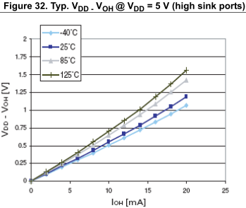
| STM8 GPIO characteristic |
Bare in mind that it is for up to 8 segments leaving less than 2.5mA per segments. I would have needed a driver in the old days. Thankfully even the cheap Chinese LED are efficient. The overall power of the display and the STM8 is around 20mA.
The SPI pins are set as open drain drivers and three 4.7K pull-ups to 3.3V are used for level shifting and isolation. That was the theory.
It turns out the "Slope Control" circuit fires up a P-Buffer for a cycle even in Open Drain mode. When the firmware detects the main supply is off, it bypasses the LED refresh code. This reduced the SPI leakages and dropped STM8 standby power from 5mA to 2mA.
The VDD rail can be backup using a supercap and/or a battery. The regular CR2032 won't work as its voltage would sag below 2.8V at 2mA drain.
A 1F supercap would in theory gives me around 13 minutes of backup.
t = (C*dV)/I where I = 2mA, C=1F, dV = (4.7V - 0.3V - 2.8V) = 1.6V
Tthe 2mA exceeded the datasheet1mA max discharge rate, so the lifetime and backup time would be reduced.
I reused the case of a Caller ID for the clock. The I/O connectors are mounted on a PCB supported by a standoff.
I broke out the Power, SWIM, Serial, I2C and a GPIO to a set of 0.1" headers. I kept the original caller ID PCB for mechanical support and connected to the traces for the buttons.
The hardware is completed at this stage.
I'll have to work on the firmware and that'll take a while. There are additional features that I want to work on. The user interface code have to be rewritten due to limited amount of information that can be displayed.
Go to part 2
Files: https://github.com/FPGA-Computer/LED-Clock
I reused the case of a Caller ID for the clock. The I/O connectors are mounted on a PCB supported by a standoff.
 |
| I/O connectors at the back side of the case |
 |
| Wiring the PCB to the I/O panel and supercap |
 |
| Clock is assembled |
Go to part 2
Files: https://github.com/FPGA-Computer/LED-Clock

