Search This Blog

Tuesday, August 7, 2018

RT5350 "3G" Router Firmware

Projects / Original post date:01/22/2015

This is a bit out of date and probably no longer needed.

I bought one of those 3G routers for $9 from China with free shipping. Same as the one talked about in detail here:http://my-embedded.blogspot.ca/2013/12/mini-4g-router-rt5350f.html except it has 32MB of SDRAM and a different firmware load that have only 10 commands when you telnet into it.This project is how to generate a custom firmware for it.Files are at https://github.com/FPGA-Computer/RT5350.git

Firmware: OpenWrt "Barrier Breaker" r35407/LuCI Trunk (svn-r9946) Kernel version: 3.7.5snapshot images are not built by default (fixed) https://dev.openwrt.org/ticket/18712

I google and played around with several precompiled firmware images for it, but I wasn't happy with any of them. They all seem to be missing a package or two as the router has only 4MB of SPI FLASH.

Here is a firmware builder for this router. https://code.google.com/p/rcc/source/browse/trunk/projects/rt5350_mini_router/OpenWrt-ImageBuilder-ramips_rt305x-for-linux-x86_64.tar.bz2

Basically this is the final pass for the OpenWRT building process when everything including all the packages have been precompiled. The scripts loads up the packages specified and compress a firmware image for it.

There are a few things that wasn't mentioned: The commands inside the scripts were compiled for x64 only, so you need to run that on x64 Linux. (I ran bodhi-3.0.0-rc2 (Ubuntu) in VirtualBox on my windows machine as it is the only x64 box I have. I had to replace the command line parameter (in text) from 16M to 32M inside vmlinux with a hex editor. The file was hardcoded for 16MB of SDRAM and it ignores the u-boot arguments. The directory path is "build_dir/target-mipsel_r2_uClibc-0.9.33.2/linux-ramips_rt305x/" Thankfully the build scripts compresses the file from scratch (as evidenced from the file date), so I don't have to figure out what to modify.

I didn't have much luck making a new entry as there is some dependency on the directory structures, so I simply modified one of the entries in the build script: "image_builder_rt5350.sh" located at the root of the package. This builds a wifi router with luci web interface and has opkg and USB mass storage support. The original factory firmware is more slick than that. I wish I had a backup :(
mini_luci_web_wifi)
    PACKAGES="opkg $LUCI $MASS_STORAGE $WIFI"
#   PACKAGES="$LUCI $DEFAULT_EXCLUDED $WIFI"
;;
To compile for it, I simply type in ./image_builder_rt5350.sh mini_luci_web_wifi

There will be a wall of scrolling text for a minute and the script spits out the compiled image at bin/ramips/mini_luci_web_wifi.bin The default ip address can be changed by editing the line containing the following line in build_dir/target-mipsel_r2_uClibc-0.9.33.2/root-ramips/etc/config /network : option ipaddr '192.168.100.1'

There are not much of space left on the SPI FLASH after the packages. If you need more file space, you can mount Rootfs on External USB Storage. The packages required are in this firmware.

OpenWRT Documentation: http://wiki.openwrt.org/doc/start
OpenWRT page: http://wiki.openwrt.org/toh/unbranded/a5-v11


TUSB Blaster


Projects /
Original post date:07/31/2014

This is an old hack that I did years ago. These days, you can buy Altera USB Blaster clones for less than $3.


I want to start playing with Altera FPGA software, but my old Byte Blaster parallel port dongle won't install under Windows x64.I dusting off my old project and make my USB Blaster clone. This is slow, but not a couple of weeks waiting for a $6 clone arriving from China slow. So this will be my back up plan if the dongle DOA or come in late.This is designed around a TI TUSB3410 USB to Serial chip which TI uses in their programming dongles for the MSP430 series. This was also popular in earlier mobile phone serial interface dongles until cheaper chips like PL2303 clones flooded the market.It has a non-enhanced 8052 core running at 2 mega cycle/sec (24MHz/12) and requires multiple cycles per instruction.This was a demo for the TUSB stack. It is as mongrel as it can be and it shows the power of Open Source very nicely.Source code:


USB device stack:
Micah Dowty wrote the pure polling USB code which I changed into interrupt + polling using 3-4 of TI App notes and use header file from libusb for the data structure. I strip off most of TI's callback functions that are hard to understand. The resulting code works kind of like V-USB and work well under SDCC.

USB_JTAG:
The hight level code came from ixo.de : http://ixo-jtag.sourceforge.net/#usb_jtag
usb_jtag project that uses Cypress FX2 which is a modern day 48MHz 8051 chip. The code was nicely optimized and with machine code for the 8051. I changed the low level GPIO bit banging code and grafted the high level code on to my USB stack.

USB Blaster:
The USB_JTAG code there was ported over to Microchip on this Japanese page: http://sa89a.net/mp.cgi/ele/ub.htm for making the Altera USB Blaster clone.

I ported the EEPROM code and USB descriptor code which are critical for cloning Altera USB Blaster back.

Hardware:

TUSB3410 connection - bus powered

Power supply and EEPROM (not actually used)


Level Translation:


Level Translation:

VIO is the I/O voltage of the target.  It comes in via series resistor R20 to power the level translation circuits.  Q5 is a shunt regulator.  It clamps down the I/O rail to limit the voltage to about 3.4V if you connect VIO to say a 5V system.

Note: U1 has an absolute maximum suply voltage of 6.5V, it is only spec for up to 3.6V for normal operation.

For the signals going out of PCB, it passes through U1 which acts as a level translator.   If my target operates on 1.8V, U1 would be on a 1.8V power supply and its output would be between 0V to 1.8V.  The 74LVC series is great for that as its logic input can exceed the power supply voltage.  There are series terminating resistors on the output to reduce signal reflection as the dingle is usually connected to a target using loose wires.

Note: 74LVC part is very fast and they require terminating resistors if your track is longer than about 0.5 inches!

Now what about the extra bits of transistors circuits?

Q4 (in Cascode topology) is a level translation circuit that convert the incoming TDO back to 3.3V for the TUSB3410.  The capacitor C7 is for compensating for Miller capacitance that would otherwise slow down the circuit.

Q2 & Q3 forms a bidirectional level translation for the TMS/SDWIO.  (SWDIO and SWDCLK are for ARM debugging not needed for USB Blaster Clone)

Jim Hagerman wrote a paper "Two Transistors Form Bidirectional Level Translator"

www.hagtech.com/pdf/translator.pdf

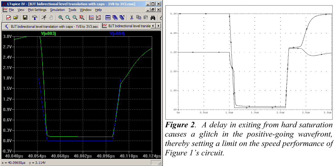
" Tests show  that the circuit operates easily up to 300kHz. The major impediment to fast operation is the delay that occurs when Q1 comes out of saturation on a rising edge."

I played around with the circuit in LTSpice and figured out how to improve the performance by adding a couple of capacitors that speeds up the discharging of the Miller capacitance that caused the slow down.

(My LTSpice circuit on left)


LTSpice plot: Blue: 1.8V input, Green: 3.3V output.

I played with the pull up values to improve the rise time. Notice that the delay is gone as the capacitor C1 discharged the Miller capacitance.  By the way, my simulation is for 10MHz!


This is how it looks like translating from 3.3V down to 1.8V


How is this useful vs the usual ones built with MOSFET circulating on the Internet?

e.g. 2N7002 has Vgs threshold of:  0.8V (min), 2.1V (typ) and 3V (max).

You'll have a bit of trouble using that part with that wide spread of a range of a threshold  for level translation.  The BJT transistors have a input threshold of around 0.7V with a much smaller spread, so it can easily work down to 1.x volt range and not limited for 3.3V.  I/O voltages are going down these days and 3.3V is only the first stop.

This is just here to show that discrete bidirectional level translation can be done using discrete parts that I have lying around.   For any logic translation, I would not recommend this circuit as it has a very high input capacitance that would load your circuit at high frequency.   There are much better bi-direction translation chips these days.

I also would not recommend this for I2C translation as this circuit does not work on open drain signals as my pull up is too small for that and the extra capacitance would make the signals looks worse.   Jim Hagerman's design uses 10K pullup and probably has that in mind.

Newer design (see epilogue):


Here is the level translation circuit I used in a more recent design.  I  deciphered the part markings and found some 74CBT1G125 parts that I can recycle.

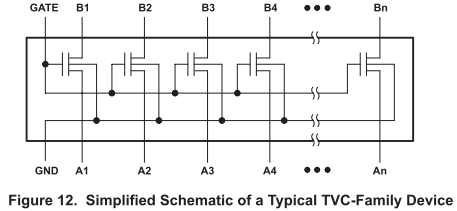
Normally these 74CBT series are designed for 5V to 3.3V level translations, but there is a way to hack it.  In one of the app note, "Table 3. Possible Voltage-Translation Combinations Using a TVC Device", TI left a bit of cookie crumbs in the bracket.


So what is inside one of these TVC?  It is simply a array of MOSFET that have their gates tied together.  What's so special about that vs discrete parts?  Since these transistors are on the same chip, their properties are very closely matched and they have the same temperature.

One of the transistors is (A1/B1) that is used as a shunt regulator to set a reference voltage at "GATE" to Vt+VREF.  If there are any process variations, this arrangement will cancel out the differences as the GATE voltage is tracking Vt.


Now what can I do for mine? If I tie /OE to ground, the inverter would connect the GATE to the supply rail making the three connection available.  Since the /OE signal doesn't change, I can assume that as long as my supply voltage is higher than Vt, that the inverter would operate statically as it should be.


I made some assumptions that the threshold voltages of these parts are probably below 1V (see hint 2) and may be with a spread of 20% due to process/temperature variations.


For my application, I set my GATE about 1.1V above the VIO and if I do see that extra few hundred mV isn't going to bother my TUSB3410 much.

I'll try to post the files up somewhere once I figure how to do so and get the code cleaned up.

Now why was I interested in bidirectional level translation?  I was planning ahead for ARM SWD debugging when I initially designed the circuit.  That's another story.

Epilogue

Recently, I built a new rev. using ATMega8 with the proper level translation chip for CMSIS DAP and hope to use V-USB. Unfortunately the CMSIS DAP code insists on using a large fixed sized interrupt transfer for HID and there is where V-USB breaks.  First off the USB standards increased the interrupt intervals from 1ms to 10ms and only allow 8 byte packets for interrupt transfer. There was no other way to send more than that either.

I rewrote part of the TI USB stack to handle the interrupt transfer needed for HID and got it partially talking to the debugger.  It was funny to see that the much slow TUSB chip chucking along as it has USB hardware and not limited by that.  The lower level stuff was mostly written for ARM, so porting wasn't going well.  Also I don't want to actually debug that stuff.  I am shelving that until I can find some $1 ARM chip.  Now that's for a different project.

OpenOCD went overboard with their code allowing accepting only FTDI devices, so I no longer interested in this nor their code base.

My code is on github: here

STM32F103 Breakout Board

Original post date:07/03/2015

I bought some STM32F103 a couple of years ago and had been procrastinating on using them. You know the usual excuses: can't make the PCB, compiler toolchain is hard to setup etc.

Now I have unused board space for a Chinese PCB batch for a job, so it is time for a speedrun for a breakout board filler. Plain breakout boards are no brainer, so that why they are perfect for these.

This is also a not so serious attempt for me to not read the datasheet in detail. What can possibly go wrong? Will this be ended up being a Fail of the Week post? Stay tuned.

SMT alert: 0402 and other small parts.

Not competing with $2 Chinese clones as they can sell it including shipping far cheaper than me asking for shipping while giving it for free. https://www.aliexpress.com/wholesale?catId=0&initiative_id=SB_20180807105855&SearchText=stm32f103c8t6+board

Here is where you can find Arduino for it if you are into that type of thing.

https://www.hackster.io/rayburne/maple-mini-clone-update
https://github.com/rogerclarkmelbourne/Arduino_STM32/wiki
https://github.com/MakerLabMe/STM32_Arduino_Cores
http://www.stm32duino.com/

Project files for my initial PCB built is on my Github directory I have cleaned up the layout a tiny bit.

I need to fill a last minute board. That was 6:30 pm last night. Between dinner and layout, etc I had it mostly (99%) done just before I went to bed at 1:15am. Now I have to play around a bit with the board outline etc. I guess I am kinda late as it is Saturday in China.

Snapshot of what I have so far:


The board came out a bit cleaner than I thought it would be. I managed to untangle the I/O ports so that they are ordered to their bit ordering instead of the pin numbering. The break out is designed for IDC cables and the usual "Dupont" loose wires cables from China should fit quite well too.

Force of habit, I try to maintain as much ground plane as I can and bridges the discontinuities the best I can. That is something not often done enough for Open Source work.

The usual 3D money shot! Usually I do this before ordering the PCB, but this is a speedrun. Good luck pressing that reset button without poking your fingers out!


Not too bad for something that I throw together in less than 24 hours.

They updated my order with the one that has the text on the correct layers. This was received on Saturday 4th July while some of us are still recovering from Canada Day and other Southern neighbours are celebrating their Independence Day.


And they have to mess up the custom value declaration again and ignore my explicit instruction to not to include shipping charges into the value. It is DHL, so there are no cheap way of getting around it. This is for work so I use the more expensive shipping option. The postal system is unpredictable and slower, but does offer refund if I can show corrected paper work.

$15 to DHL to refile the paper and possibility of bumping the shipment out to next week. (Friday today)
Pay the $21 or so for their mistakes and hope to get the supplier to refund. Ha! They haven't even reply to my email on their their shipment custom value declaration mess up.


I think I baked it a bit too much. Still trying to get used to the new hot air tool. It is a bit too bulk to hold and can blow off the small parts easily.

There was something fishy about initial power up. Might ave been a short or something. Once I desoldered the LDO and hooked up my bench supply with current limits, it powers up. Soldered back the LDO. Current is about 11mA. Sounds reasonable.

I'll leave the testing for another day as I am behind my schedules.

So looks like I might have missed the USB pull up. Pretty much most of the microcontrollers I have used have internal pullups for the USB data pins, so I don't usually think about that. The quick fix is to connect a 1.5K between PA15 and one of the USB data lines depending on the connection speeds.

Another possibility is to have a permanent 1.5K pull up on D+ to 3.3V like V-USB. The USB pins can be mapped back to GPIO and the D+ pin can be driven to logic "0" to fake a disconnect.

Blinky LED - first sign of life

I have managed to compile ChibiOS 3.0.0 for the STM32F103 using the modified Maple Mini files. I got a blinking LED running in a Thread, so the base RTOS is working.

There is something funny about the UART serial driver not initializing correctly and cause an exception error. I haven't spent much time on that as I merely copying the high level init code from my FPGA board.

Okay. That was embarrassing. The demo code was using a different driver "object" SDU1 instead of SD1 that I have initialized. So a NULL reference to SDU1 caused an exception error. Now I have to hunt down the baud rate setting. Not sure how I soldered in a 10MHz crystal instead of 12MHz.

The demo code with a simple shell is running.


Test setup:
UART1: Port A - GPIO 9: TxD, GPIO 10: RxD

Upper left Jumper: Installed = run, Not installed = STM32F boot loader.
Upper left corner: USB - Serial dongle
Upper right: SWD connector to debugger (PA13, PA14 GPIO pins are used as SWD.)


I ported my Noka 5110 LCD driver code to the board. This is using the STM32F103 SPI1. I am using the polling call as DMA overhead might be a bit too much for transferring very small blocks of data. I am going to do more coding to turn it into a ChibiOS stream device for chprintf().


Github file: here


Masks and other useful tricks in Eagle CAD

Projects / F103 Pod  Original post date: 04/29/2018

The default DRC file for OSH Park does not have solder mask for pads or vias. If you want to have a solder mask over your vias, you can change "limit" to the maximum via size that you want solder mask:


Here are some of the layers in Eagle that you might not have cared about:


Here is how I use them for making PCB footprint for a Dome momentary buttons.


I normally have all my vias with solder mask on, so I want to selectively override the vias inside the dome footprint.  To change the option, simply select the via and right click for "Properties"

Select the "Stop" to add a stop mask for the via (i.e. leave the copper bare).  Notice the difference between my regular vias (without the shade areas) and the highlighted one.


Eagle complains if I draw a via directly over the center of the dome button as it overlaps the "pin" for the footprint.  So I place a via off center and move it afterwards.

Misc

  • I draw a donut circle (in tDocument layer)over my vias so that I know how much clearance I need to leave around it.
  • I define my cream layer to reduce the amount of solder paste (60-70%) for my QFN footprints.  This fixes the issue of the QFN package floating on the solder paste of the center pad.
  • Draw a thick line in Restrict layer for high voltage vs low voltage circuit isolation.  The width of the line should the creepage requirement for the working voltage.  DRC will warn you about violation and copper pour would avoid the area.
  • Clearly label the high voltage and low voltage areas on your PCB.  It might save a life.

See here for an explanation


Add the Restrict in your opto-isolators/relays/Ethernet transformer footprints. This help DRC flag your isolation violations.  Don't run traces between rows of pins between a high voltage and low voltage circuit.  The spacing between the pins are for safety and isolation, not for routing.


Lots of layout on the web have violates this last one.  Do yourself a huge favour, unbookmark/unlike/unfollow those sites.  Don't learn bad habits from someone who don't care about the basic safety rules.

GDB DebugWire

Projects /  Original post date:05/23/2018

A self-contained GDB Server for AVR DebugWire on a $2 STLinkV2 dongle. It is loosely based on "Black Magic Probe" firmware.

DebugWire is a proprietary hardware debugger interface available on some of the ATMega series.  It is based on a half-duplex asynchronous serial protocol first documented here by RikusW back in 2011.


The DebugWire interface:


Note: There are no voltage translation logic in the cheap dongles, so the interface is only good for AVR part running at 3.3V - 5V.

How is this project different?

This work is loosely based on Black Magic Probe to create the firmware for a $2 standalone STLinkV2 clone dongle.  The firmware implements a USB CDC ACM device, GDB server and DebugWire procotol. The dongle communicates directly with GDB over a USB virtual serial link.

There are no hardware to build. This does not relies on additional packages such as OpenOCD or Python or OS specific software like some of the other projects. 

STLinkV2 Hardware

The generic STLink V2 clone is based on a STM32F103 or in some cases STM32F101.  The dongle is a hardware debugger for ST ARM Cortex series (SWD) and their 8-bit STM8 (SWIM).

5V compatibility:

All the I/O signals on the STLinkV2 clones are hardwired to 3.3V. The I/O are TTL level compatible and 5V tolerant.

For the AVR /RESET pin functioning as DebugWire (i.e. I/O)
At Vcc = 5V, VIH3 = 5V x 0.6 = 3V (min) which can be satisfied by a 3.3V signal. 


The signal I am interested in is SWIM_RST ("RST") which will be used as the DebugWire signal (/RESET).


The GPIO mapping shows that it is connected to both Timer 3 and USART1


The USART1 will be used in half-duplex mode with the pin configured as Open Drain which is compatible with DebugWire as is.  PB5 will be configured as weak pull-up (input).


The Timer pin could be used to monitor the pulse width of the Break signal from the AVR to determine the communication speed.

There are other signals such as SWIM, SWCLK, SDIO on the dongle.  They might be useful as a SPI programmer and/or wired for serial printf() at some future point.

Useful links

https://github.com/dcwbrown/dwire-debug - useful reference for implementing DebugWire commands

Tear down

I opened up my STLinkV2 clone and soldered to the SWD.  The pads are specific to this PCB and may be different for your clone.  Pin from Left to right:  SWDIO, GND, SWCLK, +3.3V 
The pads are 0.05" pitch which matches the spacing for a ribbon cable.

(I have traced the connections with my multimeter and looked up the datasheet.)

This is what the back side looks like.  VUSB is routed directly to the 5V on the connector.  There is a PTC fuse (F1) in the VUSB rail for 5-pin 3.3V regulator (U1) that powers the F101 and connected to the 3.3V pins on the connector.  There seems to be a reasonable amount of decoupling caps on the regulator as well as the microcontroller.

22R series resistors (R1, R2) are used for the USB data pins, but populated a 1K pull-up (R3) vs the 1.5K specified by the USB standard!  There are 22R series resistors (RP1) on the connector signals.


They are using a STM32F101CBT6 part in my STLinkV2 clone.  They'll use the cheapest parts they can source for a production run, so don't expect the same parts or same PCB.


The F101 officially does not have USB device functional block. It turns out that there is SRAM at address 0x20000000 - 0x200004FFF which works out to 20KiB (instead of 16KiB).  I don't have to worry too much trying to squeeze in the code/data size for testing.


Dongle ProgChip masks are expensive, they are probably economizing by using the same dies from their big brother(s) with the "missing" features left untested. For a high volume matured part, the yields should be pretty high so these features would likely to work untested. On the other hand, some of these chips might have been binned because their extra features failed.

Make that you have two STLinkV2 clones on your shopping list.  You would need an additional STLinkV2 programming anyways.  Do not update the dongle you want to use with STLinkV2 firmware as it might enable Read Protect.

SWD pinout for some of the clone variations: here

Unlocking Read Protect for STM32F10x

Seems like the STM32F101 chip is read protected because of DRM on the STLink firmware.  This is probably because I updated it to their latest firmware as an initial test for the dongle.  The read protect feature protects the FLASH memory outside of code access as well as write protects the first few blocks.  A full chip erase does not disable the read protection in the option word as the unlocked values is not 0xFF by design.


Steps
1. Perform a Chip erase


2. Change the option byte


At this point a window will popup.  Select "Disable" and hit "Apply"


After a progress bar, this warning popups.


3. "Disconnect" from target and then "Connect" again. 


4.  If you are not getting the following screen, you might have to repeat steps 2-3 one more time.


The read protect on the chip is now disabled!

What I did earlier trying to figure out the bootstrap mode.   Don't bother with this unless you are looking for punishment.

I desoldered the chip to see if there are hidden connection.


Boot1 (PB2) is already shorted to GND on the PCB, so don't need to do anything.
Boot0 has a 10K (R5) pull down to GND.  Pull this pin to 3.3V for serial bootstrap.


USART1 TX (PA9) is connected to the LED.  It is accessible from the right  pad  of R9.


They could have made break out the USART1 RX with a test pad on the right side, but they didn't.  You'll need to solder a fine wire to pin.  So this is not the right way for anyone else.  

I have decided to try something else and eventually got it working with the STLink Util.   It wasn't mentioned in the first few google search pages.  Who would have thought it was that simple!