https://www.reddit.com/r/diyelectronics/comments/4j3hl9/winner_advanced_challenge_buck_regulator_olympics/
Congratulations to /u/fpga_computer for his winning entry! This entry features the 2nd place (adjusted for mounting type) cost, 1st place efficiency, and a tremendous write-up on hackaday.io!I saw @oshpark post about Buck Regulator Olympics contest on reddit /r/diyelectronics earlier today. I guess I can't help being interested in this contest. I actually have a lot of discrete boost converter designs, but no buck converters.
Entry submitted. Elapse time: about 24 hours including design/built/documentation/test.
This is what I have so far for a high frequency reasonably efficient discrete buck converter with fast transient response. The contest allows comparators, so that's what I am going to be using. See bottom of the page for full schematic.

Control Circuit
I am making a voltage mode hysteretic buck converter. The output voltage of the regulator is compared against a 3.3V reference.U2 is wired as a comparator with hysteresis with R3 is the series resistor and C4 for positive feedback. C4 injects a large amount of positive feedback that is only active once the falling/rising edge transition started. This ensures that the edges are fast and clean and a minimum on/off time. The feedback soon disappear allowing the comparator to compare voltage accurately.
 |
| Comparator feedback current via C4 |

Power circuit
I am going to use a P-MOSFET with a discrete gate driver. Q1 & Q2 forms a pseudo push-pull driver. I am using a 3A schottky diode as the free wheel diode.The following shows the MOSFET gate voltage and current.
 |
| Green trace: Gate voltage, Blue trace: Gate current |

Most of the power losses are when the MOSFET switches on/off and not I^2 *R losses. The switching edge is where the voltage * current is the greatest. It is critical to switch the MOSFET as quickly as possible to minimize the time in the transition. So this is the case where a large MOSFET with low Ron would be worse. You want to pick a MOSFET with low gate charge so that it can be switched quickly and use a gate driver circuit correctly sized for it.
The circuit is delivering 3.3V^2/2R = 5.44W, average MOSFET power loss: ~0.1W (~2%) That's not too bad for an old SOT23 MOSFET. :)

Power loss for the 3A diode: 0.423W

Changing to a 5A diode actually makes it worse. Once again, bigger isn't always better.

Power loss for inductor: CD75-100

There is a high power loss because of the low duty cycle (high input, low output) so the diode conduct 63% of the time. At 5V input when the duty cycles is higher, the diode loss is reduced to 0.122W while the loss at the MOSFET rises to 0.233W
So far the overall power loss is: 0.1 + 0.423 + 0.218 = 0.741W The rough estimate of this design to be somewhere below 88% efficiency at 12V (Vin max) which is the worse case for this design.
Transient Performance:
In LTSpice, I attached a current source to the output of the supply to provide a load step of 1.5A (0.1A to 1.6A) with 1us rise/fall time to test the output load step response. I don't have a fast transient load tester to test this. May be some day, I'll build one.The output undershoot to 3.21V (-0.09V -2.7%) and overshoot to 3.49V (+0.19V +5.7). Not a lot can be done about the overshoot as the load drop except to use a large value capacitor with lower ESR.
V(n006) is the MOSFET switching node.

Zoom in view:
The fast response of this type of converter can be seen here. The duty cycle pretty much changed right away. (0V means on for P-MOSFET). The output slew rate is only limited by the L & C.

From Linear Tech App note 149 on fast and stable loop.

I guess I got c).

The current limiting seems more trouble than it is worth. I'll leave that for the time being.
Work to be done is a 3.3V reference source out of discrete. The lowest part count approach is to use a 3.3V Zener and manually trim the output voltage by an adjustable constant current source.
R9 and C5 is used to implement soft start (slew rate control) to limit the inrush current as the buck converter would otherwise try to charge the output filter cap as quick as possible. In the case of a hysteretic buck converter, it will try to stay at 100% duty cycle.
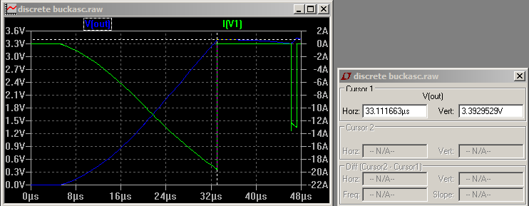
With R9 and C5. The inrush is about 2x nominal.

Zoom in view:

This is without soft start. The MOSFET is driven to 100% duty cycle until the output reaches set point. Huge inrush current!
Preliminary results
Here is the quick proto using perf board and copper tape with what I have on hand. I used a micro coax cable for both the feedback and ground reference to the control circuit at the output terminals.I haven't got around to the reference circuit in this picture. I wired up a 3.3V zener diode and 5.6K resistor to +12V for initial testing.

This is the final design with reference circuit:

Here is the output ripple for 12V input, 2R load. It is about 104mV. I used a cap with ESR of 0.125R for cost reasons. A low ESR cap would also reduce the output ripple.
The switching frequency is quite a bit off from 300kHz , but it is still in the sweet spot for these type of components. The difference is probably due to component tolerances and for L & C which can quite large.
 |
| Output ripple under 2R load |
 |
| P-MOSFET gate voltage |

I did some more work designing the reference circuit. The Zener is used as a reference for biasing itself. The output voltage of the Zener is multiplied by 2 using the otherwise unused comparator in the package (with R7 pull up) as opamp.
- The voltage at the comparator output (wired as a non-inverting amplifier) is 3.3V * 2 = 6.6V.
- The voltage across R6 is 6.6V - 3.3V = 3.3V. The zener output voltage can be tweaked by changing R6 to adjust the value of the constant current. The value was determined to be 720R empirically for my Zener diode. I used 220R + 1K//1K = 720R.
 |
| Zener reference |
Load Testing
My collection of load resistors in case you can't see them clearly. 15R, 2R and 3R.
Load regulation: no load 3.31V

With 2R (4R//4R)

With 15R load (220mA)

With 33R load (100mA)

Full schematic

Efficiency:

Note: not a whole lot of significant digits for the low current ones, so take that with a gain of salt. My estimated efficiency number for full load are spot on! :)
BOM
Digikey US prices for comparison.
I have all the parts in my collection and some at cheaper price from China. I got the CD75-10 from Aliexpress. The efficiency shows that they work as well as the Sumida part.
LTSpice Simulation files: github
This is what the layout would look like. The proto on perf board works well enough.
It is done as single sided for home prototyping The secondary side if present is a ground pour. The power component placements are based on minimizing current loops. C2 is used as a bridge between the 12V/Gnd for the AC return path when Q3 turns on to drive MOSFET.
The comparator takes its feedback and ground reference near the output connector JP2. Board size: 30.76mm x 24.13mm

Optional C9/R9 snubber not installed. It is easier to have the footprint in case you need it.


Would I build this for practical use? No, there are much better $0.40 modules I can buy. It is a good exercise to learn about designing a power supply.
Discrete 5V/10A Synchronous Buck Converter
Original post date:11/14/2016This is a follow up to the Discrete 3.3V Buck Converter project log. I do not intended to build this as is because there are chips that can do a better job and offer fault protection. Due to the discrete nature of this design using easy to find models, it can be useful for running under LTSpice (or other simulators).
At one point for the Reddit contest, I thought about adding short circuit protection by sensing current going through the diode D1. The control circuit is a bit complicated and not worth the extra BOM cost to earn a design feature. It'll take a few discretes and would be a lot easier if I can throw in some 74HC parts. The contest rule doesn't allow for that. It is one of those things that a chip could have done it smaller, cheaper and more efficiently.

The control circuit is a result of the 3.3V design but with a proper 2.5V reference (e.g. TL431) (once again because I am not constrained by contest rules.) R9 and C5 are for slowing down the initial rise time to limit the inrush current. R9 can be increased to slow down the slew rate for real life. ~0.8ms might be too fast for some, but great for speeding up simulation time.
I am using a synchronous rectifier (M2) to minimize the conduction loss in this design. It is driven off the output of comparator U2. I added (R10, D5, C7) and (R8,D4,C2) on the control signal to introduce a delay to minimize cross conduction between M1 and M2 during cross over.
I am using a N-MOSFET for the main driver so that I can use N-MOSFET. It comes at a cost of complexity. Q5 inverts the polarity of the signal and R8, D4 and C2 provides the necessary delay. A charge pump (C1, D6, D7 and C6) leeching off the H bridge is used to provide the high voltage for driving M1. The duty cycle to below 100% to keep the charge pump going. An external driver supply can extend the operation to 100%.
The blue trace shows the gate voltage of M2. The red one shows the gate voltage relative to the source for M1. The delay between the two signals is to prevent cross conduction. D1 picks up the slack during the cross over. Because of the low duty cycle, I get by with a 1A schottky diode. There are more intelligent gate driver parts with control schemes such as Predictive Gate Drive (TM) and Adaptive Gate Driver that can squeeze another few percent of efficiency by tightening the timing and better gate driver circuit to minimize the losses due to slow switching.

The power components values are picked based on what I have on hand. In general I like to balance the losses between 3 parts: M1, M2 and the discrete to roughly the same amount for more bang per buck. (pun intended)
M2 is chosen for low R(ON). The power loss is 1.35W at full load of 10A

In this case I am using the old 20N03 for both parts because I got a pile of them from scrap boards and it is just good enough for this design. The power loss for M1 is 1.82W.

A copper pour larger than 0.5 square inch should be used to dissipate this amount of heat. You really don't want to use the TJ = 150C (from graph) for a design.

These are the power components for this design. A fill under these parts is close to 1 sq inch. You are going to want heavy copper pours and traces to carry the high current anyway. Vias to power planes on the solder side can help to dissipate power.

A better gate drive could improve on this as the losses are during switching. You want to switch this part as fast as you can with lots of gate drive. In contrast, M2 losses are due to I^2*R.

The green trace is the gate current for M1 and blue for M2. Red trace is the H bridge output. The simple discrete gate driver design is at its upper limit for this MOSFET due to high gate charge. Just using a gate driver chip could easily improve on the efficiency and allow for higher power.

The losses for diode and inductor (Coiltronic HC1-5R1) is 0.54W. I haven't account for the filter caps and misc. they'll probably be in the 0.2W range depending on the ESR.

So for a 5V 10A output, the losses is around 1.35W + 1.82W + 0.54W + 0.2W = 3.91W.
Efficiency = ~ 50W / (50W + 3.91W) = ~92.7%.
Simulation files are on github. There you have it...
may i know the reason of multiplying the reference voltage to 6.6V?
ReplyDelete