Search This Blog

Tuesday, February 14, 2023

STM8 - Generating 2 phase PWM

A push pull converter uses two drivers that are 180 degrees out of phase.

It is possible to generate PWM on 2 channels that are 180 degrees out of phase in  TIM1on a STM8S003.  All the register settings are from the reference manual, but you won't find an example.

TIM1 is set up as an up/down counter in Center-aligned mode. This spaces out the 2 phase PWM signal evenly.

Since the timer is counting both up and down in 1 PWM cycle,  auto-reload value for TIM1 should be set as 1/2 of the value to generate PWM frequency. I used TIM1_FREQ of 27kHz in my code.

#define CPU_CLOCK 16000000UL
#define TIM1_FREQ 27000L
#define TIM1_PSCR 1
#define TIM1_CLK (CPU_CLOCK/TIM1_PSCR)
#define TIM1_ARR (TIM1_CLK/TIM1_FREQ/2)
#define TIM1_PSCRH ((TIM1_PSCR-1)>>8)
#define TIM1_PSCRL ((TIM1_PSCR-1)&0xff)
#define TIM1_ARRH ((TIM1_ARR)>>8)
#define TIM1_ARRL ((TIM1_ARR)&0xff) 

// Clk = 16MHz
CLK->CKDIVR = 0;
 
TIM1->PSCRH = TIM1_PSCRH;
TIM1->PSCRL = TIM1_PSCRL;
TIM1->ARRH = TIM1_ARRH;
TIM1->ARRL = TIM1_ARRL; 

// TIM1 enable, Center-aligned mode 3
TIM1->CR1 = TIM1_CR1_CEN|TIM1_CR1_CMS; 

Output enable (and polarity) bits of the corresponding TIM1 channels can be set in TIM1 CCERx.  I use CH3 and CH4.

// CH3, CH4 output enable, polarity active high
TIM1->CCER2 = TIM1_CCER2_CC4E|TIM1_CCER2_CC3E;

From the Reference Manual:

110: PWM mode 1 - In up-counting, channel 1 is active as long as TIM1_CNT < TIM1_CCR1, otherwise, the channel is inactive. In down-counting, channel 1 is inactive (OC1REF = 0) as long as TIM1_CNT > TIM1_CCR1, otherwise, the channel is active (OC1REF = 1).

PWM Mode 1 when ARR =8 and CCR = 4

PWM mode 2 works similarly, but with the output polarity inverted.

111: PWM mode 2 - In up-counting, channel 1 is inactive as long as TIM1_CNT < TIM1_CCR1, otherwise, the channel is active. In down-counting, channel 1 is active as long as TIM1_CNT > TIM1_CCR1, otherwise, the channel is inactive. 

One can generate a PWM signal using a sawtooth wave and a comparator.  


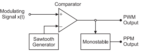
PWM generation using analog circuit - Sawtooth wave and a comparator

The modulating signal level is the CCR value, the TIM1 counter is the sawtooth wave. The PWM modes 1 and 2 are just the polarity setting on the comparator.


PWM generation using TIM1

 One of the TIM1 channel (CH3) is set up with PWM Mode 1 while another channel (Ch4) as PWM Mode 2.

// CH3: PWM mode 1, preload, output
TIM1->CCMR3 = (6<<4)|TIM1_CCMR_OCxPE;
// CH4: PWM mode 2, preload, output
TIM1->CCMR4 = (7<<4)|TIM1_CCMR_OCxPE;

Use PWM Mode 1 for one of the channels to center an output around Timer count = 0 and Mode 2 on the other to center around Timer count = ARR. This is how you can generate the 2 phase PWM signals.

The CCR values could be set independently. In some applications, you want them to have the same PWM duty cycles. The granularity of the PWM signal is 2 TIM1 clocks. (125ns in my code)

void Set_PWM(uint16_t Value)
{
Value >>=1;
// CCR3 = n/2
TIM1->CCR3H = Value >>8;
TIM1->CCR3L = Value & 0xff;

// CCR4 = TIM1_ARR - n/2
Value = TIM1_ARR - Value;
TIM1->CCR4H = Value >>8;
TIM1->CCR4L = Value & 0xff;
}

Turn on the MOE (Main Output Enable) bit in TIM1 BKR (Break Register). An external signal can be used to disable the TIM1 outputs in the case of a hardware fault. e.g. over-current or over-temperature condition

// Master output enable
TIM1->BKR = TIM1_BKR_MOE;

This are some the output of PWM waveform at 27kHz captured on my logic analyzer.

2 phase PWM at 27kHz

Set_PWM(2) - 27kHz close to 0% duty cycle

2 Set_PWM(294) - 27kHz close to 50% duty cycle

Sunday, February 12, 2023

Optocouplers

Optocouplers are some of those things that are deceivingly easy to a beginner, but also hard to use correctly.  If you are reading the datasheet carefully, you are in for a big surprise.

CTR (Current Transfer Ratio): sensitivity of the coupler - the ratio of the transistor output current vs the LED current.  e.g. for a 50% CTR, you have to drive the LED with 10mA and the transistor switches 5mA.

The CTR spec is very loose and likely this series of optocouplers are just different bins of the same parts.  They don't even include a max value.  


This ones show both min and max value from 100% to 200%. The following shows the part to part variation of a for a small samples of a (different) optocoupler.

CTR of a small sample of PS2021 optocoupler

Analog feedback

The optocoupler is commonly used as an analog feedback in an isolated power supply.  The error voltage is pass back as a current sink or source to close a negative feedback loop of a regulator across a voltage barrier.

I played around with the isolated power supply design from previous blog with feedback from the secondary side.  The voltage regulation is very tight and virtually stays at around 5V from 5mA to125mA load.

I have no idea on how well it would work with the loose CTR specs.

Passing digital signals

They are one of those things that was made with compromises. In order to make the device sensitive, they made a big photo-transistor at the expense of large parasitic capacitance (Millar Capacitance) and and suffers from slow speed.


Reference: Vishay has a great app. note on Faster Switching from Standard Couplers.  It covers all the technical stuff.

It'll be pretty sad day if I don't try to make something slow to go fast. I played around with LTSpice and came up with something that is not covered by the app. note.  

The values I used are determined by the optocoupler CTR.

Optocoupler circuits: simple, medium and complex

To see their performance, I put them side by side and feed each of these circuits with the same 5 pulses of 100kHz signal (200kbps data rate).


Top trace: Input (cyan), bottom traces outputs from optocoupler circuits

Simple coupler circuit (green)


CBC  (base collector capacitance) aka Millar Capacitance. It slows down the transistor. Datasheet typically uses 10V and a load resistor of 100R as their test circuit.  CBC is low at higher voltages and the small pull up value help with the rise time.

Note: the scale from Low to high (left in log scale) is very different from High to low (right in linear)

The speed is much slower when you use a large pull up resistor and lowering the voltage. The values I picked is might be useful for low data rate may be lower  tens of  kilobits per second. e.g. asynchronous serial.  It should only be used with a Schimtt Trigger input to clean up the slow rise and fall time.

The middle circuit (blue)

The optocoupler is the first stage of inverter that drives a  transistor of a second stage inverter.  Its output range is clamped to a diode drop of the transistor base voltage. The operating point is not a good spot for low CBC. 

Input (Cyan), Q1 base voltage (Purple), Output (Blue)

In spite of that, it only take about 100mV change in base voltage for the transistor to turn on or off.  It is a good compromise to squeeze an extra bit of bandwidth out of the old optocoupler. There is a bit of inconsistency in the timing. A timing analysis should be made for setup/hold time for protocols that require coordination of multiple signals e.g. SPI.

The more complex circuit (Red)

It bypasses the Miller effect as it uses the transistor junction as a photo diode. The comparator threshold is set to about mid point of the input (~100mV). The speed (propagation around 500ns) is limited by the $0.20 LM393 type of comparator that is used to amplify the signal.

You can speed up the photodiode even more by using a transimpedance amplifier.  Because of the feedback, the voltage across the diode junction is maintained around 0V, the switch time is greatly minimized.  However  high speed amplifiers cost more and I don't have a whole lot of them.

Nowadays, there are specialized devices with active circuit to make them go fast. e.g. high speed logic gate coupler, IGBT/MOSFET gate drive coupler. Some of them uses capacitor or magnet coupling.  There are isolation devices for USB, I2C.  These are the ones that are too messy to to roll you own.