Search This Blog

Friday, September 20, 2019

Canada Post SUX

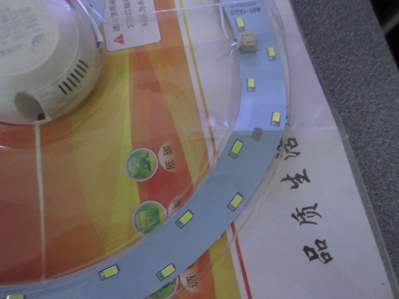
Once again, the local delivery person from Canada Post destroyed my package.

LED ring has metal backing, cardboard package with plastic.

It was bent really badly
enough to break the PCB traces
All this is because the local delivery person decided to bent the package trying to force it inside my mail box.  It is not like the community mailbox is more than 8 feet away from the mail room or that the person has to fill a 10 page forms to do it.  The person ended up doing it when he/she founds out that my package wasn't quite bendable.  By then it is too late.

Canada Post doesn't list an email contact on their website.  The only way is via social media.


Out of those, Twitter was the least invasive.  Not going to sign up with the rest.

I have decided to try to talk to a person.  It is hard as most companies don't want you to talk to them.  I filed a complain.


Monday, September 2, 2019

USB meter modding - Part 2

I have further modified the USB meter to improve on the voltage and current resolution by more closely matching the input range to the full scale of the ADC.


Here are the additional modifications:

Additional modification to the PCB

For 10V input, the ADC sees: 10V * 4.7K/(1.2K + 10K + 4.7K) = 2.956V which is just shy of ADC 3.0V full scale. Even for the native 10-ADC, I should be able to get to 10mV resolution.

For a 2A current, the ADC should see around 2A * 0.01R * (100+1)/1 = 2.02V.  For the native 10-bit ADC, I should get about 3mA resolution. I am extending the ADC resolution using oversampling.

The Opamp has a negative DC offset (Vos), so it cannot read low currents.  The part also have a somewhat high temperature coefficient as it drifts. There are at least 2 different pin outs for opamp that I am aware of. The TLV2461 from TI matches this part.
.
opamp pin out

It is not the first choice I would have picked because of its negative Vos (offset voltage) around ground.  This negative Vos if not corrected can drown out low current measurements.  The Vos has a curious shape of 3 distinct sections.  This is typical of rail to rail input opamps as it actually have both ground rail and supply rail input section for the full supply range.  Each of these front ends have their dominating Vos in its operating regions. Around mid rail is where they sort of cancel out each other.

Vos vs input common voltage
The saving grace is that this part is that the Vos has a low temperature coefficient. The unknown part used has a lower Vos, but I have seen it drift.

Temperature coefficient: 2uV/C

I have added a 2M2 resistor to add a DC offset.  This offset get multiplied by the gain of the amplifier (101X). Now the output is around 63mV with 0mA load.  This DC will be taken care of by the calibration.

New: I had a lot of issues with the current measurements jumps all over the place. I trace it down to poor grounding in the layout.  They use a thin trace to connect the ground. This same thin track is shared by the LDO which supplies the microcontroller. The voltage drop on the trace changes as the LED segments are lit and this gets amplified by the current sense amplifier.  There is also a tiny bit of DC offset between the opamp ground and the microcontroller which introduce about 2-3 LSB of offset.  I added a couple of 24AWG wires (shown in purple) and they help to reduce the amount of jitters in the raw measurement. I also have a sliding window averaging as a low pass filter to stabilize the readings.

Replaced USB cable, improved grounding and SWIM for debugging
I improved on the grounding with the 24AWG wires in black marked in purple lines in the mod guide.
I have replaced the flimsy USB cable with 2 twisted pairs from Ethernet patch cable in sleeving. The wires are 24AWG which can carry up to 3.5A safely. Unfortunately these cable weren't meant for soldering, so there are some solderability issues. I had to use some heat shrink tubing to cover the easily melted insulation. I drilled a bigger hole in the plastic molding from the original cable.

From https://www.powerstream.com/Wire_Size.htm


SWIM connector for debugger
I superglued a connector on the PCB and made a cut out on the case for the debugger. This should make life a bit easier in the long run.

For calibration, I modify the display routine to show the raw ADC value which I then input the data into a spreadsheet for linear regression.

Regression analysis of raw ADC values vs input voltage
The coefficients are then converted to fractions approximation for scaling the ADC values for the results. This let me work with integer math as it is much faster and take up less space.

Note: The website no longer exists.  Use this High Precision Decimal to Fraction online calculator


After the preliminary calibration, the measurements are within +/- 1 digits of my multimeter. I probably need to redo this as I have improved the grounding and that shifted the offset slightly.

Multimeter in voltage mode
Multimeter in current mode
The mod seems to be able to see current down to 1mA.  I ran into a bit of non-linearity issues as the current gets higher due to heating effects on the traces and sampling resistor.

As larger range is used for the analysis, the higher currents affects the otherwise linear data at the lower ranges. Using the 0 - 0.604A coefficients, I get +/-1 mA for 0-500mA, but the values gets to +/-2 above that.

Residual plots of different current ranges
One way to avoid this is to use piece-wise fit as it'll allow much closer fit to a subset. As shown below,  the residual is within +/- 1 for 0.653A - 1.065A.


The higher current ranges has a reduced display resolution of 10mA, so I could get by with extrapolation from the 1A curve.

The specs after calibration:
  • Below 3.20V, "LO" (Low) is displayed. Above 10.19V, "OV" (Over Voltage) is displayed
  • 3.20V - 9.99V : +/- 0.01V.
  • Current display: 0-999mA +/- 1mA with zero suppression. 1.00 - 2.00A +/- 10mA.
Additional ideas:
While there are no free I/O pins, the column drivers (CC2..CC6) could be re-purposed for reading push buttons. They are programmed as open drain output.

Inside the TIM2_Update_IRQ( ), the 5 inactive column drivers can be reprogrammed into the "Input pull-up" configuration using the CNF1 and CNF0 registers.  Push buttons in series with a 4K7 series resistor can be used to pull these I/O to '0'. The resistors limits the current to minimize display artifacts.


Alternate display format can be used for additional data e.g. min, max voltage/current, power measurement.

The hardware UART pins are used for ADC and cannot be shared. One of  the segments (e.g. Decimal Point) into a 3V UART transmit pin.  The timer compare functions could be used for more precise timing needed for bit-banging.

I have decided to make a small adapter PCB for the microcontroller.


It probably going to take 3 weeks.  Available from https://oshpark.com/shared_projects/nWySOWYk
Link: Part 1, part 3

Project file: https://github.com/FPGA-Computer/USB-Voltage-Current-Meter
The option bytes are default  (0x00)

Option byte setting

Saturday, August 31, 2019

USB meter modding - Part 1

USB meters can come in handy for measuring the voltage and current. While they may have 3 digits display, some of them do not actually have the resolution nor are calibrated.

This is a mod for a $2 USB meter to to improve on the resolution and accuracy closer to my digital multimeter with the added bonus of much lower voltage drops. My modifications and calibration (part 2) makes up for the loose tolerance parts.

Modded meter reads 13mA (3mA for the LCD meter + 10mA for serial dongle)
The LCD meter cannot see the dongle even though the current is within range.
I have decided to modify one for an impulsive weekend project. It is a KW203 from a few years ago for about $2. The ones I saw are overpriced ($10-$20) and you can get really fancy LCD ones for about $3.

It uses a SO18 wide package, so a replacement microcontroller can be fitted within the footprint.  It is simple enough that the I/O mappings can be traced.

PCB with microcontroller removed.
The current measurement is done with a 0.01R sampling resistor placed in the ground connection between the input and the USB connectors. A SOT23-5 opamp in a non-inverting configuration provides 48X gain.
The amount of voltage drops is lower than the average multimeter.

The voltage measurement is done with a voltage divider of 15K in series and 2K to ground.  There is a ceramic capacitor in parallel to provide the low impedance for the ADC.

There is a group of 5 resistor footprints behind the "Charger" USB connector.  They are to provide the "Charger" voltage divider for Android/iOS charger.

There are foot prints for a couple of SOT23 sized trimpots for both measurement, but they are bypassed with a couple of 0 ohms resistors jumpers instead.

There is a MD78U30 3V LDO to provide a 3V rail for the microcontroller as the meter is supposed to be able to handle 3.2V - 10V.  There is a small 10uF tantalum bulk decoupling cap on the output rail. There are no additional decoupling caps provided.

Cheat sheet I used for wiring up the microcontroller
The two IC are the old and the replacement microcontroller.  I have decided to use the STM8S008F3 as it has just the right number of I/O needed: 14 I/O for driving the 6 digits multiplexed 7-segment LED display and 2 ADC inputs for the measurements. If I scale the input correctly, the 10-bit ADC, I should be able to get close to 3-digit resolution.  I am using oversampling to improve on the resolution, but the actual resolution depends a lot on the noise floor and type.

There are a few gotchas:
  • PB4, PB5 are "True" Open drain pins, so they can only be used for the common cathode and not the segments. PA1, PA2 are standard GPIO vs the rest of the HS (High Sink), so those segments might be slightly dimmer. 
  • There are no series resistors, so the LED is current limited by the GPIO driver resistance.  The power rail is set at 3V which helps a bit. The LED switching can affect the ADC reading as the ADC has no internal reference and use the power rail as reference.
  • There are 3 ceramic caps for this part. VCAP is the 1.8V decoupling cap for the internal regulator, and one for the 3V rail. The NRST can probably be ignored, but I connected it per datasheet  recommendation.
  • There are no spare I/O. The SWIM pin is also used in driving the first digit and its GPIO function is disabled when the debugger is connected.
  • The 7 segment display only have decimal point at the first digit.
  • The grounding isn't good and 4-wire connection isn't used at the sampling resistor which can affect the linearity at higher currents.
The part is small enough to fit within the footprint. This is a quick and dirty hack, so I am not going to make a custom flex PCB at OSH Park and wait for it.

Replacement microcontroller soldered
I soldered in the microcontroller with some fine magnetic wires and even wired in the required capacitors on top of the chip.  The extra wires are the SWIM, NRST pins for the hardware debugger/programmer.

Test display
After a bit of debugging, I got the timer IRQ to turns on the column driver and dumps out the corresponding digit stored in the buffer at a refresh rate of ~59Hz.

So far the I/O seems to be going to the right places and the hardware debugger works. The current drawn is about 10.5mA.

Project file: https://github.com/FPGA-Computer/USB-Voltage-Current-Meter

  • I found a KW203 reverse engineering article here after my mod.
  • There are also panel meter with a STM8.
  • I have seen one of the more LCD fancy one last week and it seems to be using a 20-pin TSSOP microcontroller. 


This one might have a STM8S003 and a 4 pin programming connector.

Thursday, August 15, 2019

XVCD rev2 - part 1

I tried implementing a JTAG programmer for Xilinx devices using the ESP8266, but I wasn't happy with the overall design - Arduino, bitbang JTAG, 2.4GHz WiFi etc.

There is a problem with the XVC protocol is written.


Normally the TMS vector needed is a lot shorter to get a device into programming mode while the bulk of the programming data is handled in the TDI/TDO.  The protocol expect that both the TMS and TDI vectors are output to the device while receiving the TDI in one go. While this provides the maximum flexibility, it is the part that causes a bottleneck on the performance.

I though using the SPI would have improved the situation, but I guess I didn't read the fine prints carefully to realize that I need to have both outputs.

I am in the process of working on my new design using a popular cheap but capable STM32F103.  It is the same size as the ESP8266 module and consumes a lot less power.
3D model
Top side
Solder side
I am using both SPI in the STM32F103 part for the JTAG interface.  SPI1 acts as the master SPI (for TCK, TDI, TDO) while SPI2 (for TMS) is the slave.   Both the SCK are wired together to synchronizes the two SPI.
SPI1 and SPI2 are used to drive the JTAG signals
 .
ST wired the SPI2 to the AHB1 clock domain (36MHz) which limits the overall data rate to 18Mbps instead of the 36Mbps supported by SPI1. The bottleneck in this design is Full Speed USB (12Mbps).

My bare metal (i.e. no libraries) SPI DMA + interrupt code works on first try! It is probably a lot easier (for me) than baby sitting the 3 SPI data stream and keeping them well fed with firmware loop.  It also frees up the CPU for the rest of the code.


The SPI is set up for 8-bit transfers using 3 DMA channels for each of the vectors. A bitbang routine handles any left over bits.  It is hooked to the DMA completion IRQ and takes 3us for the switch over. The bitbanging is at  1.8Mbps which is 1/10 speed of SPI, but it only need to deal with at most 7 bits of data.


The next hard part is dealing with Windows, USB and the networking stuff.

Friday, December 21, 2018

STM8 Timer - Irrigation

Projects / Misc 8-bit uC projects

Water level sensor

The TPP223 (.pdf) touch sensor I bought finally arrived.  As usual, the LED is just too bright.  I change the series resistor (bottom in black) to a 2K (0603).  A small value capacitor (0-50pF) can be added to the empty footprint at the top right corner to reduce the sensitivity of the sensor.

The default output is push-pull, active high, non-toggled.
There are two solder bridge jumpers: A, B to set the following options.
A: (AHLB) pin 4 - Active low
B: (TOG) pin 6 - Toggle


For testing, I used a small piece of double side tape to stick it to the side of a plastic container and slowly filling it with water.  The LED lights up for a minute or so.


I think this could be useful for determining if water level reaches the high water mark.

I cut up a plastic bottle into two halves and fitted the top end with a short PVC jacket from a stranded CAT5 patch cord.  I used lots of hot glue to seal the joint. The top end works like a funnel. I drill a hole on the bottom half for the exit.


I tried to make a gentle L bend without crushing the PVC jacket.


I am trying to avoid using regular tapes as they tends to dry up and crack under sun light. I cut up 3 strip of paper about 2" wide x 11" long.  I applied a generous amount of white glue and use it to wrap it around the plastic bottle to hold it together.  This forms a paper mache shell to hold the two halves together.


I soldered in a 22pF capacitor to the empty pads on the touch sensor board.  This lowers the sensitivity a bit. I soldered a short piece of wire (~1cm) to the corner pad of the touch sensor to a small copper foil.  The bottom part of the copper foil is used to set the high water mark.


The output of the board drives a 2N7002 MOSFET which converts it to an Open Drain output.  This will be wired in parallel to the light sensor.  The on resistance of the MOSFET is about 10 ohms.

I have to make my trip much sooner. I have given away two of the plants as I can always grow more.  Only been running it for a few days on the remaining one and it seems to be okay.

Things I have learnt so far:
  • The pump I used is a centrifugal pump which requires that the pump to filled with water.
  • The pump produces a lot of electrical noise generated by the DC motor during commutation to reset the microcontroller.  I have included ceramic cap near the output connector on my PCB, but that wasn't good enough.  I had to add a 0.047uF cap at the pump side end of the long cable. I added another one to the other end of the cable for good measure.
  • The water drains out of the container very quickly making it hard to measured..  There are ways to stop the drainage.  Right now I set the timer for a fixed time instead of relying on water level detection
  • There was water leaking out of the seams in the pump, so I touched it up with super glue. That fixed the issue.
  • Water from the container relies on gravity.  Some water droplet ends up sticking to the small diameter silicon tubing.  It amounts to less than a couple of cc.  Try to keep he slope of the tubing uniform to minimize the water retained. I might try using a slightly larger diameter tubing. It probably not going matter too much as they'll get pushed out next time.