Search This Blog

Sunday, January 12, 2020

STM8 LED Clock - Part 2

Go to Part 1

The regular AT-cut crystal has a temperature variation that can be modeled by a cubic equation. Variations from the ideal angle produces the following curves centered around 25C.

AT - cut frequency-temperature characteristics.
If the temperature variation is small enough, then a regular AT-cut crystal might be good enough.
e.g. home with heater during the winter set to 21C and air conditioner set to 25C for the summer. The temperature variation is roughly 4C.

 For a wide temperature range or lower temperature dependency, you might want to use a TCXO (Temperature compensated crystal oscillator).

There are a few  ways of making an accurate clock out of an oscillator:
  1. Use an external accurate clock source and/or resync. the time e.g. GPS or internet time
  2. Try to adjust the clock frequency of the oscillator by changing the load capacitance. This is difficult and the adjustable range might not be enough.
  3. Try to compensate for the tolerance by changing the frequency divider.
I am using the last approach as it is the least expensive and provide a finer repeatable adjustment than what is possible a trimmer capacitor.  The CPU clock is divided down to generate IRQ for the software real time clock.

In my Timer project, I used a hardware timer set to overflow every 60,000. By changing this value,  I can tweak the IRQ by ~ 1/60000 which should be good enough for +/-0.72 sec/day accuracy after calibration. 

This time, I generate a 20Hz IRQ and further divide down the frequency to 10Hz for the RTC using a 24-bit Numerically Controlled Oscillator (NCO). The NCO allows for very fine frequency.adjustments.

The 3 lines NCO code is actually much simpler than the firmware that would be required to extend the hardware timer divider beyond 16 bits.
DDS Code
So far I have calibrated the clock by simply comparing when the clock changes vs https://time.is/ - whether it is faster or slow and by using a binary search algorithm to find the value. This doesn't require any additional coding or equipment, but it takes a bit of time.

The latest calibration is less than +/-1 sec/month after 7-8 turns of such adjustments.  I measured 1 second difference after 4 weeks 6 days.

Additional Reference:
User Interface
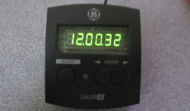
The clock and display time:
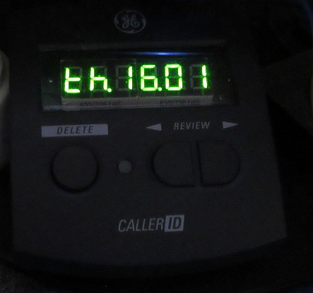
The arrows key switches between the time and date display.  The date display uses a different format to distinguish the modes.  The 7 segment LED can only show a limited set of characters and have to make the closest approximations. 
e.g. Th(ursday) 16 Jan is shown below.
The user interface is still work in progress as the display is very limited. Here is how to set the time.
How to set time
Alternately, Hold the Menu for ~1 second to exit the setting mode.

Go to Part 3 for my new alarm clock.

Sunday, November 3, 2019

STM8 LED Clock - part 1

I always wanted a VFD clock, but the tubes I have that can fit inside the case I have only have 4 digits. I have recently bought some green 7 segments display that I can find from China. There wasn't any data, but they were cheap. They turn out to be a bit bigger for something else I had in mind, so I might as well put them in good use.
Clock in reused CallerID case
I used a 74HC595 for driving the LED segments. I could have rearranged the GPIO in USB Meter modding to reshuffle the pins for external crystal. 
LED Clock PCB
The I/O assignments are for ease of routing on a single sided home brew PCB. The toner transfer wasn't ideal, but I managed to get it to work.
Segment driver
This driver circuit is on a separate power supply away from the STM8 isolated by D1.  This makes it easier to control the brightness and power backup. 
Power supply
The problem working with undocumented parts is that you have no idea how much current they need until you are committed. I have originally planned to use a zener diode and NPN transistor. 

Luck would have it that 3.3V gives me the right brightness while not overloading the STM8 GPIO used as common cathode driver. I ended up using a XC6206P332MR LDO as it is cheaper than the zener diode + transistor

STM8
The STM8 circuit is pretty boring. GPIO PB4-5 and PD4-6 can be used for expansion. There are 6 common cathode drivers which double up as button inputs and power sense.

The button pulls the pin low via a 10K series resistor (to avoid display artifacts).The firmware changes the GPIO pin to an input with internal pull up during polling. The input supply is sensed via a voltage divider such that leakage voltages (SPI to Vin via the LDO parasitic diode) if present is less than the VIH threshold.

Buttons and Vin sense
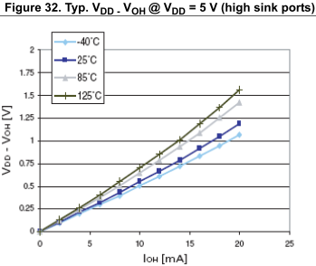
STM8S003 has a minimum operating voltage of 2.95V and it resets below 2.8V. So a schottky diode after the 3.3V LDO would not leave much headroom. Also the I/O have higher current rating at 5V. 

STM8 GPIO characteristic
Bare in mind that it is for up to 8 segments leaving less than 2.5mA per segments. I would have needed a driver in the old days. Thankfully even the cheap Chinese LED are efficient. The overall power of the display and the STM8 is around 20mA.

The SPI pins are set as open drain drivers and three 4.7K pull-ups to 3.3V are used for level shifting and isolation. That was the theory.


It turns out the "Slope Control" circuit fires up a P-Buffer for a cycle even in Open Drain mode. When the firmware detects the main supply is off, it bypasses the LED refresh code. This reduced the SPI leakages and dropped STM8 standby power from 5mA to 2mA.

The VDD rail can be backup using a supercap and/or a battery. The regular CR2032 won't work as its voltage would sag below 2.8V at 2mA drain.


A 1F supercap would  in theory gives me around 13 minutes of backup.
 t = (C*dV)/I where I = 2mA, C=1F, dV = (4.7V - 0.3V - 2.8V) = 1.6V 

Tthe 2mA exceeded the datasheet1mA max discharge rate, so the lifetime and backup time would be reduced.

I reused the case of a Caller ID for the clock. The I/O connectors are mounted on a PCB supported by a standoff.

I/O connectors at the back side of the case
I broke out the Power, SWIM, Serial, I2C and a GPIO to a set of 0.1" headers. I kept the original caller ID PCB for mechanical support and connected to the traces  for the buttons.

Wiring the PCB to the I/O panel and supercap
The hardware is completed at this stage.
Clock is assembled
I'll have to work on the firmware and that'll take a while.  There are additional features that I want to work on. The user interface code have to be rewritten due to limited amount of information that can be displayed.

Go to part 2

Files: https://github.com/FPGA-Computer/LED-Clock

Friday, October 4, 2019

USB meter modding - Part 3

The PCB I have ordered from OSH Park arrived.

PCB vs original SOIC-18 microcontroller
The milling wasn't completely perfect, but it is good enough for my needs.  The drill hole is small 0.0197" (0.5mm). One side of the milling was at the mid point of the hole which is the edge of my outline.

Some of the copper were removed by the milling
The goal of the tiny PCB is to replace the hand wired mod.
Hand wired mod vs PCB
I taped down the PCB for soldering/hot air reflow.
I used 3 pieces of "Kapton" tape tohold down the PCB.
Side view f the solder joints
PCB soldered. Blue wires are for SWIM programming
It's alive!
Links: Part 1, Part 2
PCB can be ordered from https://oshpark.com/shared_projects/nWySOWYk 
It is a 2 layers 0.031" (0.8mm) thick PCB

Project file: https://github.com/FPGA-Computer/USB-Voltage-Current-Meter

Friday, September 20, 2019

Canada Post SUX

Once again, the local delivery person from Canada Post destroyed my package.

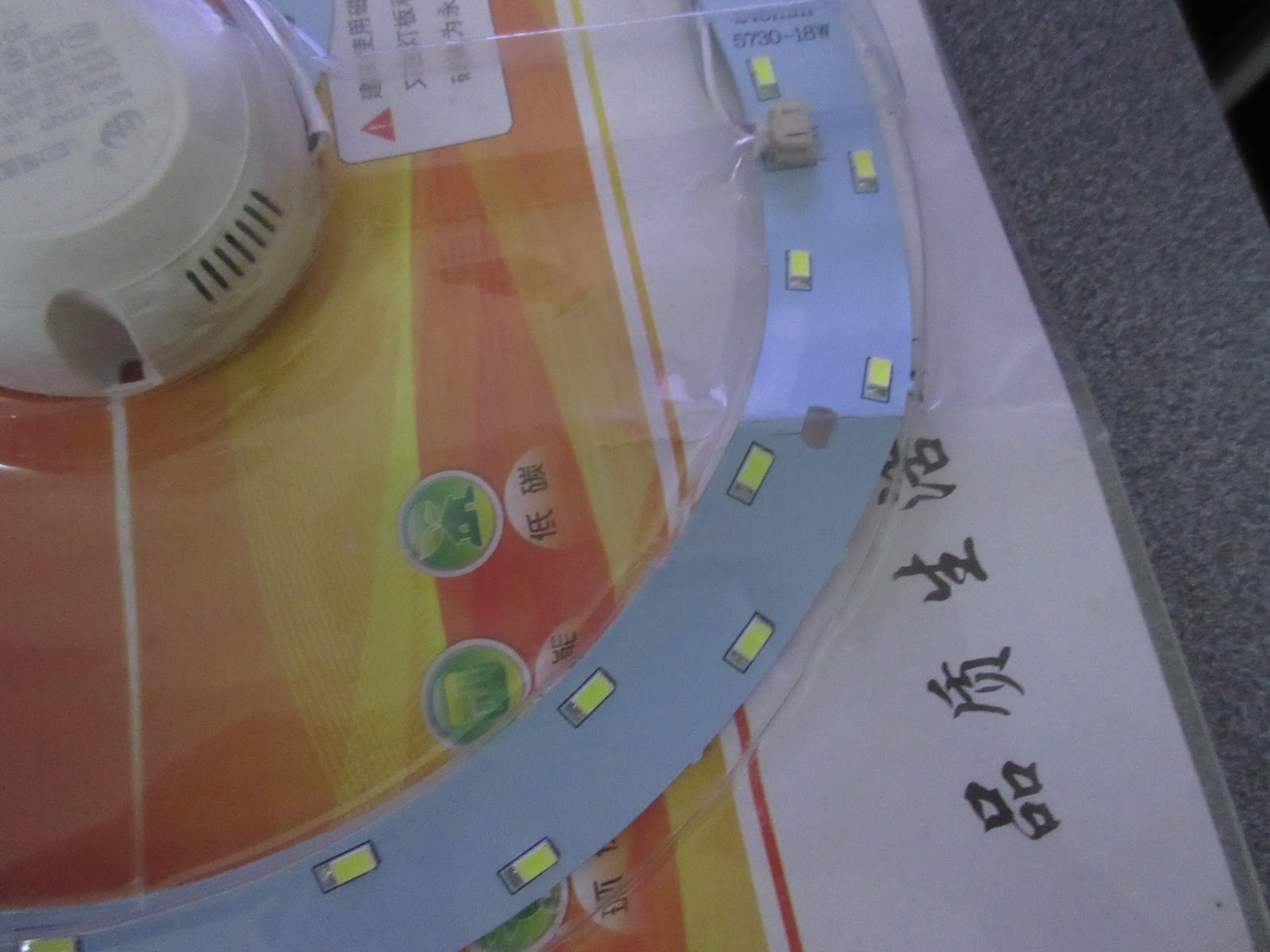
LED ring has metal backing, cardboard package with plastic.

It was bent really badly
enough to break the PCB traces
All this is because the local delivery person decided to bent the package trying to force it inside my mail box.  It is not like the community mailbox is more than 8 feet away from the mail room or that the person has to fill a 10 page forms to do it.  The person ended up doing it when he/she founds out that my package wasn't quite bendable.  By then it is too late.

Canada Post doesn't list an email contact on their website.  The only way is via social media.


Out of those, Twitter was the least invasive.  Not going to sign up with the rest.

I have decided to try to talk to a person.  It is hard as most companies don't want you to talk to them.  I filed a complain.


Monday, September 2, 2019

USB meter modding - Part 2

I have further modified the USB meter to improve on the voltage and current resolution by more closely matching the input range to the full scale of the ADC.


Here are the additional modifications:

Additional modification to the PCB

For 10V input, the ADC sees: 10V * 4.7K/(1.2K + 10K + 4.7K) = 2.956V which is just shy of ADC 3.0V full scale. Even for the native 10-ADC, I should be able to get to 10mV resolution.

For a 2A current, the ADC should see around 2A * 0.01R * (100+1)/1 = 2.02V.  For the native 10-bit ADC, I should get about 3mA resolution. I am extending the ADC resolution using oversampling.

The Opamp has a negative DC offset (Vos), so it cannot read low currents.  The part also have a somewhat high temperature coefficient as it drifts. There are at least 2 different pin outs for opamp that I am aware of. The TLV2461 from TI matches this part.
.
opamp pin out

It is not the first choice I would have picked because of its negative Vos (offset voltage) around ground.  This negative Vos if not corrected can drown out low current measurements.  The Vos has a curious shape of 3 distinct sections.  This is typical of rail to rail input opamps as it actually have both ground rail and supply rail input section for the full supply range.  Each of these front ends have their dominating Vos in its operating regions. Around mid rail is where they sort of cancel out each other.

Vos vs input common voltage
The saving grace is that this part is that the Vos has a low temperature coefficient. The unknown part used has a lower Vos, but I have seen it drift.

Temperature coefficient: 2uV/C

I have added a 2M2 resistor to add a DC offset.  This offset get multiplied by the gain of the amplifier (101X). Now the output is around 63mV with 0mA load.  This DC will be taken care of by the calibration.

New: I had a lot of issues with the current measurements jumps all over the place. I trace it down to poor grounding in the layout.  They use a thin trace to connect the ground. This same thin track is shared by the LDO which supplies the microcontroller. The voltage drop on the trace changes as the LED segments are lit and this gets amplified by the current sense amplifier.  There is also a tiny bit of DC offset between the opamp ground and the microcontroller which introduce about 2-3 LSB of offset.  I added a couple of 24AWG wires (shown in purple) and they help to reduce the amount of jitters in the raw measurement. I also have a sliding window averaging as a low pass filter to stabilize the readings.

Replaced USB cable, improved grounding and SWIM for debugging
I improved on the grounding with the 24AWG wires in black marked in purple lines in the mod guide.
I have replaced the flimsy USB cable with 2 twisted pairs from Ethernet patch cable in sleeving. The wires are 24AWG which can carry up to 3.5A safely. Unfortunately these cable weren't meant for soldering, so there are some solderability issues. I had to use some heat shrink tubing to cover the easily melted insulation. I drilled a bigger hole in the plastic molding from the original cable.

From https://www.powerstream.com/Wire_Size.htm


SWIM connector for debugger
I superglued a connector on the PCB and made a cut out on the case for the debugger. This should make life a bit easier in the long run.

For calibration, I modify the display routine to show the raw ADC value which I then input the data into a spreadsheet for linear regression.

Regression analysis of raw ADC values vs input voltage
The coefficients are then converted to fractions approximation for scaling the ADC values for the results. This let me work with integer math as it is much faster and take up less space.

Note: The website no longer exists.  Use this High Precision Decimal to Fraction online calculator


After the preliminary calibration, the measurements are within +/- 1 digits of my multimeter. I probably need to redo this as I have improved the grounding and that shifted the offset slightly.

Multimeter in voltage mode
Multimeter in current mode
The mod seems to be able to see current down to 1mA.  I ran into a bit of non-linearity issues as the current gets higher due to heating effects on the traces and sampling resistor.

As larger range is used for the analysis, the higher currents affects the otherwise linear data at the lower ranges. Using the 0 - 0.604A coefficients, I get +/-1 mA for 0-500mA, but the values gets to +/-2 above that.

Residual plots of different current ranges
One way to avoid this is to use piece-wise fit as it'll allow much closer fit to a subset. As shown below,  the residual is within +/- 1 for 0.653A - 1.065A.


The higher current ranges has a reduced display resolution of 10mA, so I could get by with extrapolation from the 1A curve.

The specs after calibration:
  • Below 3.20V, "LO" (Low) is displayed. Above 10.19V, "OV" (Over Voltage) is displayed
  • 3.20V - 9.99V : +/- 0.01V.
  • Current display: 0-999mA +/- 1mA with zero suppression. 1.00 - 2.00A +/- 10mA.
Additional ideas:
While there are no free I/O pins, the column drivers (CC2..CC6) could be re-purposed for reading push buttons. They are programmed as open drain output.

Inside the TIM2_Update_IRQ( ), the 5 inactive column drivers can be reprogrammed into the "Input pull-up" configuration using the CNF1 and CNF0 registers.  Push buttons in series with a 4K7 series resistor can be used to pull these I/O to '0'. The resistors limits the current to minimize display artifacts.


Alternate display format can be used for additional data e.g. min, max voltage/current, power measurement.

The hardware UART pins are used for ADC and cannot be shared. One of  the segments (e.g. Decimal Point) into a 3V UART transmit pin.  The timer compare functions could be used for more precise timing needed for bit-banging.

I have decided to make a small adapter PCB for the microcontroller.


It probably going to take 3 weeks.  Available from https://oshpark.com/shared_projects/nWySOWYk
Link: Part 1, part 3

Project file: https://github.com/FPGA-Computer/USB-Voltage-Current-Meter
The option bytes are default  (0x00)

Option byte setting